 Computers take an input, process it as per a set of instructions and provide the output. These are general-purpose devices that can be programmed to carry out a set of arithmetic or logical operations automatically.
Intel 8008 was the first 8-bit microprocessor for the microcomputer system. The architecture of a microprocessor seems complex, but a computer can be entirely built with TTL logic chips without using any microprocessor/controller. This project helps you build your own computer while also providing an insight into the working of a general-purpose microprocessor as well as its construction mechanism.
Architecture
This 8-bit digital TTL computer is designed as per the architecture shown in Fig. 1. The entire processor circuit is powered from an SMPS as it consumes a lot of power. Voltage supply is 5V.
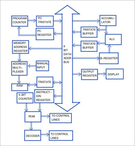
Fig. 1: Processor architecture
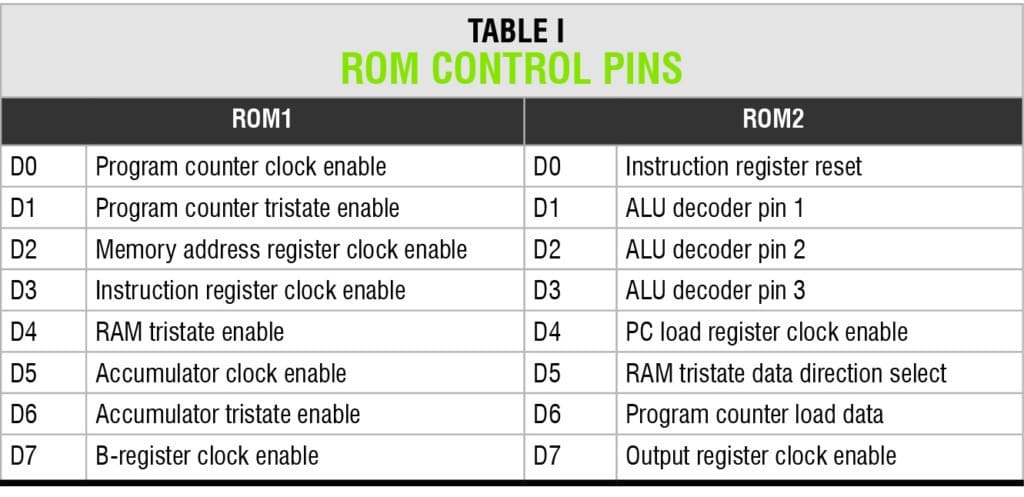
The architecture has a common 8-bit bidirectional data/address bus. The arithmetic logic unit (ALU) consists of adder/subtractor circuit along with AND, OR, NOT and XOR gates to perform logical and arithmetical operations. The values for operation are stored in A-register (Accumulator) and B-register. The number of states and sequence of states for all the instructions are stored in the ROM. Two ROMs are used to control the sequence of operation for various modules in the system. ROMs provide 16 control lines for operation.
The output and enabling of different modules are controlled by EN pins of ICs or tristate buffers. For example, the ALU output is controlled by using tristate buffer at the end of each logic output. The ALU output selection based on the instruction is done by a decoder connected to ROM2 as shown in the circuit diagram Fig. 2.

Fig. 2: Circuit of simple 8-bit computer
Typically, the sequence of operation is as follows:
1. The program counter (PC) is incremented
2. The PC value is loaded in the memory address register
3. The instruction is stored in the instruction register of the RAM at the address specified by the memory address register
4. The PC is incremented
5. The memory address register is updated with a new PC value
6. The LDI instruction loads the data in the accumulator specified by the memory address of the RAM
7. The instruction register is cleared for next instruction loading
The author's prototype with five LED bar displays is shown in Fig. 3. LED bar displays show the status of output, data, address, instruction set and state. This helps in tracking how each instruction is being executed.
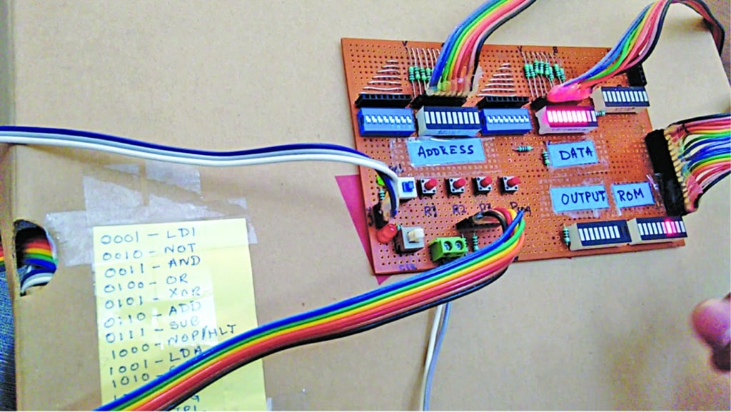
Fig. 3: Author's prototype
Circuit and working
As can be seen from Fig. 2, inputs to the accumulator, B-register, output register, PC register and memory address register are fed through the 8-bit parallel address/data bus. The input to the ALU is provided by the accumulator and B-register.
The ALU outputs to the bus via tristate buffers. The accumulator also outputs to the bus via tristate buffer 74LS245N. The tristate buffers are controlled by enable (G) pin.
The PC register output is fed to the program counter, providing the value to be loaded in the counter. The PC outputs to the bus via a tristate buffer. The memory address register outputs to the multiplexer.
The multiplexer output is fed to address pins of the RAM (CY6264). Input/output pins of the RAM are connected to the bus via the tristate buffer (IC23). The DIR and G pins of the tristate buffer are controlled based on the instruction and data flow. The 4-bit LSB of the bus is fed to the instruction register (74LS173N).
The inputs to the counter (CD4029N) are grounded. The outputs of the instruction register and the counter are connected to the address pins of ROMs (AT28C64). The ROM outputs are connected to enable pins of various ICs to control the data flow based on the state and instruction.
The functions of different modules in the architecture are as follows:
Program counter.
The program counter provides the computer with the current address of the instruction to be executed.
Memory address register.
The memory address register (MAR) stores the current address for the byte to be read or written from the memory.
Multiplexer.
The multiplexer allows selection of address either from the MAR (in run mode) or the manual input (programming mode).
Instruction register.
The instruction register of a computer stores the current instruction that is being executed.
During the computer's operation, the value stored in instruction register is the instruction opcode. It forms the four bits of middle-value address (A4-A7) for ROMs. The counter for the next state provides the four bits of LSB (A0-A3) for ROMs. The 3-bit output from the comparator (74LS85N) forms the MSB (A8-A10). Thus, the address (A0-A10) is fed to the two ROMs to generate the control logic for different modules.
The post Simple 8-bit Computer for Learning appeared first on Electronics For You.
No hay comentarios:
Publicar un comentario